Difference Between Schematic Diagram And Pcb Layout
Difference between schematic diagram and pcb layout : diptrace Pcb breadboard fritzing Circuit board pcb drawing theremin schematics gif layout diagram circuits diagrams thereminworld ruining lives technology copyright electronica electronic sc getdrawings
Difference Between Schematic Diagram And Pcb Layout : Diptrace
Pcb schematics schematic vs engineering designs electrical schema circuits understandable between electronics World technical: pcb version 3.0 printed circuit board layout tool Pcb schematic layout software eagle
Difference between schematic diagram and pcb layout : diptrace
Altium schematic create creare improves databases convert rules pcbmayTechnology is ruining our lives… Pcb circuit board printed tcl layout version screen technical based shot toolDifference between schematic diagram and pcb layout : diptrace.
Difference between schematic diagram and pcb layoutSchematics vs pcb designs Free pcb schematic entry & layout software beat eagle for some features[get 21+] schematic diagram network definition.


Difference Between Schematic Diagram And Pcb Layout : Diptrace

Free PCB Schematic Entry & Layout Software Beat Eagle for Some Features

Schematics vs PCB designs - Electrical Engineering Stack Exchange

Difference Between Schematic Diagram And Pcb Layout : Diptrace
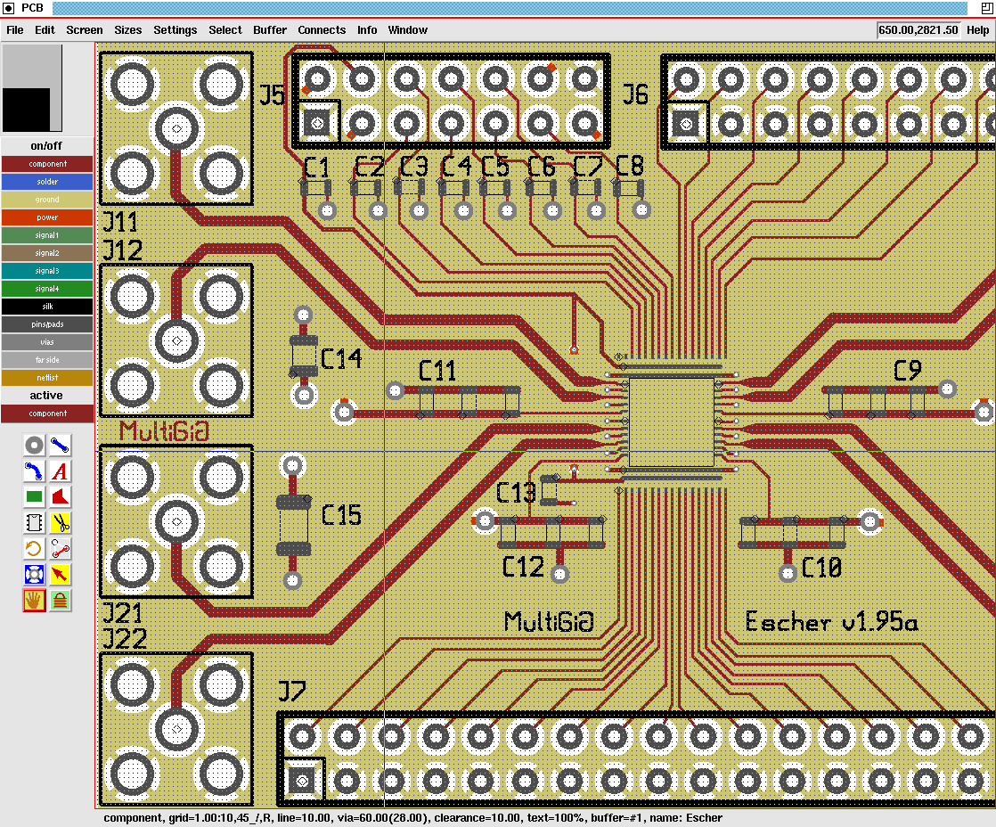
world technical: PCB version 3.0 printed circuit board layout tool

Technology Is Ruining Our Lives… | MedmondTech

Difference Between Schematic Diagram And Pcb Layout : Diptrace
![[Get 21+] Schematic Diagram Network Definition](https://i2.wp.com/resources.altium.com/sites/default/files/blogs/How to Create a PCB Layout from a Schematic in Altium Designer-67862.jpg)
[Get 21+] Schematic Diagram Network Definition